
EIR203-2SC Guide
User manual for EIR203-2SC
Table of contents
Document Outline
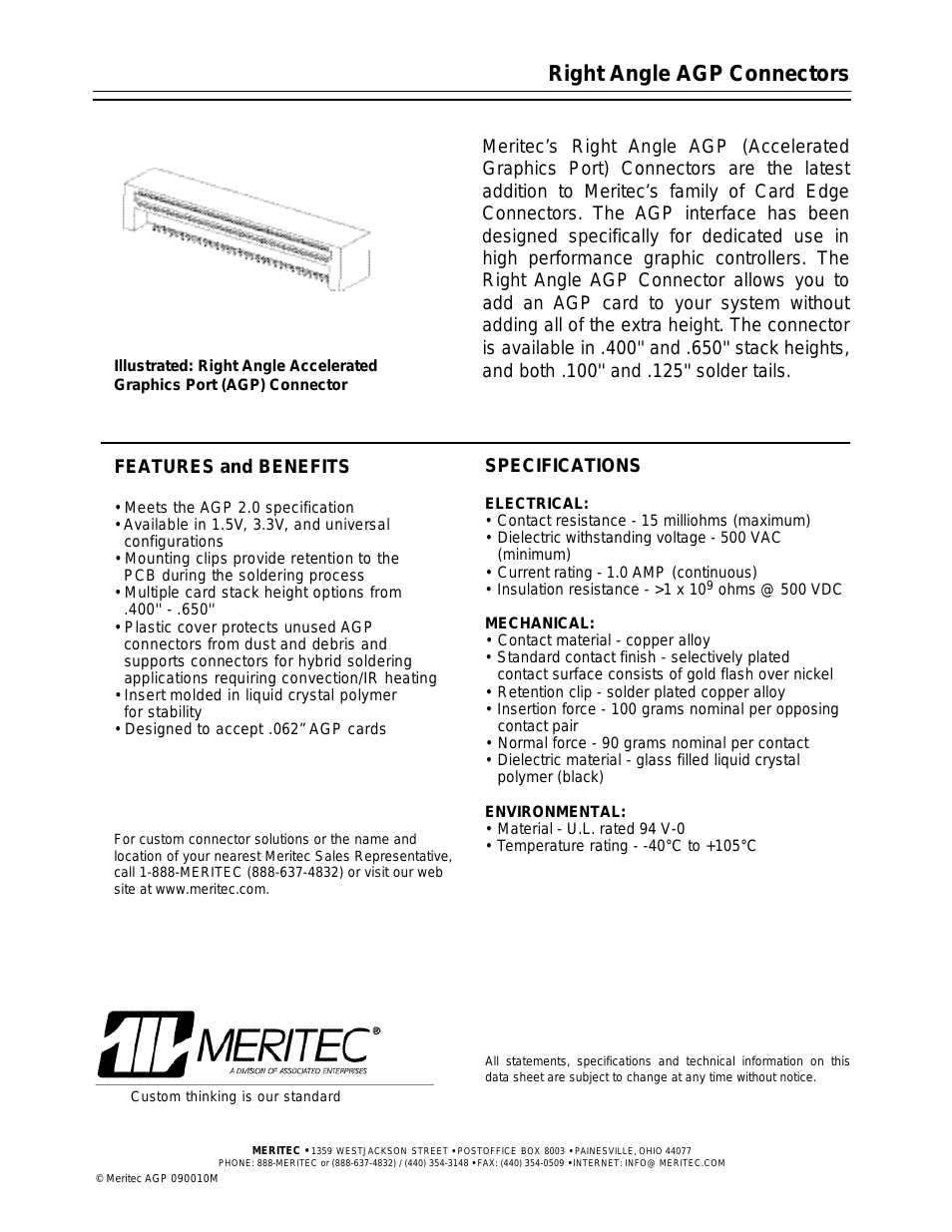
- ChapterTitlePreface - Preface
- ChapterTitle - Chapter 1 – I/O Cells
- Table - Table 1-1: Supported Single-Ended Voltage Standards
- Table - Table 1-2: Supported Differential Voltage Standards
- Heading1 - IOPAD
- Heading1 - IOPAD_D
- Heading2 - Bidirectional Registered I/O Pad with Asynchronous or Synchronous Set/Reset
- Figure - Figure 1-2: IOPAD_D Logic Symbol
- Table - Table 1-7: Ports
- Table - Table 1-8: Parameters
- Table - Table 1-9: Output Function Table (txregmode = ”reg”, oeregmode = “reg”, rstmode = “async”)
- Table - Table 1-10: Output Function Table (txregmode = ”reg”, oeregmode = “reg”, rstmode = “sync”)
- Table - Table 1-11: Input Function table (rxregmode = “reg”)
- Heading3 - Verilog Instantiation Template
- Heading3 - VHDL Instantiation Template
- Heading2 - Bidirectional Registered I/O Pad with Asynchronous or Synchronous Set/Reset
- Heading1 - IOPAD_D2
- Heading2 - Bidirectional DDR I/O Pad with Asynchronous or Synchronous Set/ Reset
- Figure - Figure 1-3: IOPAD_D2 Logic Symbol
- Table - Table 1-12: Ports
- Table - Table 1-13: Parameters
- Figure - Figure 1-4: IOPAD_D2 Output Timing Diagram (assumes txdata_en = 1’b1)
- Figure - Figure 1-5: IOPAD_D2 Input Timing Diagram (assumes rxdata_en = 1’b1)
- Heading3 - Verilog Instantiation Template
- Heading3 - VHDL Instantiation Template
- Heading2 - Bidirectional DDR I/O Pad with Asynchronous or Synchronous Set/ Reset
- Heading1 - IPAD
- Heading1 - IPAD_D
- Heading1 - IPAD_D2
- Heading1 - IPAD_DIFF
- Heading1 - IPAD_DIFFD
- Heading1 - IPAD_DIFFD2
- Heading1 - OPAD
- Heading1 - OPAD_D
- Heading2 - Registered Output Pad with Asynchronous or Synchronous Set/Reset
- Figure - Figure 1-15: OPAD_D Logic Symbol
- Table - Table 1-33: Ports
- Table - Table 1-34: Parameters
- Table - Table 1-35: Output Function Table (rstmode = “async”)
- Table - Table 1-36: Output Function Table (rstmode = “sync”)
- Heading3 - Verilog Instantiation Template
- Heading3 - VHDL Instantiation Template
- Heading2 - Registered Output Pad with Asynchronous or Synchronous Set/Reset
- Heading1 - OPAD_D2
- Heading1 - OPAD_DIFF
- Heading1 - OPAD_DIFFD
- Heading2 - Registered Differential Output Pad with Asynchronous or Synchronous Set/Reset
- Figure - Figure 1-19: OPAD_DIFFD Logic Symbol
- Table - Table 1-42: Ports
- Table - Table 1-43: Parameters
- Table - Table 1-44: Output Function Table (rstmode = “async”)
- Table - Table 1-45: Output Function Table (rstmode = “sync”)
- Heading3 - Verilog Instantiation Template
- Heading3 - VHDL Instantiation Template
- Heading2 - Registered Differential Output Pad with Asynchronous or Synchronous Set/Reset
- Heading1 - OPAD_DIFFD2
- Heading1 - TPAD
- Heading1 - TPAD_D
- Heading2 - Registered Tristate Output Pad with Asynchronous or Synchronous Set/Reset
- Figure - Figure 1-23: TPAD_D Logic Symbol
- Table - Table 1-51: Ports
- Table - Table 1-52: Parameters
- Table - Table 1-53: Output Function Table (rstmode = “async”)
- Table - Table 1-54: Output Function Table (rstmode = “sync”)
- Heading3 - Verilog Instantiation Template
- Heading3 - VHDL Instantiation Template
- Heading2 - Registered Tristate Output Pad with Asynchronous or Synchronous Set/Reset
- ChapterTitle - Chapter 2 – Registers
- Heading1 - Naming Convention
- Heading1 - DFF
- Heading1 - DFFE
- Heading1 - DFFEC
- Heading1 - DFFEP
- Heading1 - DFFER
- Heading1 - DFFES
- Heading1 - DFFN
- Heading1 - DFFNEC
- Heading1 - DFFNEP
- Heading1 - DFFNER
- Heading1 - DFFNES
- Heading1 - DFFNR
- Heading1 - DFFNS
- Heading1 - DFFR
- Heading1 - DFFS
- ChapterTitle - Chapter 3 – Logic Functions
- ChapterTitle - Chapter 4 – Lookup Table (LUT) Functions
- ChapterTitle - Chapter 5 – Arithmetic Functions
- ChapterTitle - Chapter 6 – Memories
- Heading1 - BRAM80K
- Heading2 - 80k-bit Dual-Port Memory
- Heading2 - BRAM80K Pins
- Heading2 - Parameters
- Table - Table 6-2: BRAM80K Parameters
- Heading3 - porta_read_width(portb_read_width)
- Heading3 - porta_write_width(portb_write_width)
- Heading3 - porta_write_mode(portb_write_mode)
- Heading3 - porta_clock_polarity(portb_clock_polarity)
- Heading3 - porta_peval(portb_peval)
- Heading3 - porta_latch_rstval(portb_latch_rstval)
- Heading3 - porta_en_out_reg(portb_en_out_reg)
- Heading3 - porta_reg_rstval(portb_reg_rstval)
- Heading3 - porta_regce_priority(portb_regce_priority)
- Heading3 - porta_initval(portb_initval)
- Table - Table 6-3: Relationship of porta_initval(portb_initval) bit positions to douta,doutpa,doutpxa (doutb,doutpb,doutpxb)
- Heading3 - porta_srval(portb_srval)
- Table - Table 6-4: Relationship of porta_srval(portb_srval) bit positions to douta,doutpa,doutpxa (doutb,doutpb,doutpxb)
- Heading3 - mem_init_file
- Heading3 - initd_000 – initd_255
- Heading3 - initp_00 – initp_31
- Heading3 - initpx_00 – initpx_31
- Heading2 - Memory Organization and Data Input / Output Pin Assignments
- Table - Table 6-5: Valid Port A Width Versus Port B Width Combinations per port for n x 5 width modes
- Table - Table 6-6: Valid Port A Width Versus Port B Width Combinations per port for n x 9 width modes
- Table - Table 6-7: Valid Port A Width Versus Write Port B Combinations per port for n x 2 width modes
- Table - Table 6-8: dina(dinb) bit assignments per porta_write_width(portb_write_width) values
- Table - Table 6-9: Write Enable to Data Input Bus Mapping per Write Port Width
- Table - Table 6-10: douta(doutb) bit assignments per porta_read_width(portb_read_width) values
- Table - Table 6-11: BRAM80K Address Bus Mapping (Per Port)
- Table - Table 6-12: Mapping of Word Sizes to the Native 2048x40 Memory Locations
- Heading2 - Read and Write Operations
- Heading3 - Read Operation
- Heading3 - Write Operation
- Table - Table 6-13: BRAM Output Function Table for Latched Mode (Assumes active-high clock, port enable, and latch reset value)
- Table - Table 6-14: BRAM Output Function Table for Registered Mode (Assumes active-high clock, output register clock enable, and output register reset)
- Heading3 - Simultaneous Memory Operations
- Heading3 - Timing Diagrams
- Figure - Figure 6-3: Write-First, Latched Mode Timing Diagram
- Figure - Figure 6-4: Write-First, Registered Mode Timing Diagram
- Figure - Figure 6-5: No-Change, Latched Mode Timing Diagram
- Figure - Figure 6-6: No-Change, Registered Mode Timing Diagram
- Heading3 - Support for Read-First (Read-Before-Write) Memory Operations
- Heading2 - Memory Initialization
- Heading2 - BRAM80K Verilog Instantiation Template
- Heading2 - BRAM80K VHDL Instantiation Template
- Heading1 - BRAM80KFIFO
- Heading2 - 80k-bit FIFO Memory
- Heading2 - Parameters
- Table - Table 6-16: BRAM80KFIFO Parameters
- Heading3 - sync_mode
- Heading3 - write_width
- Table - Table 6-17: FIFO write_width versus Maximum Write Depth
- Table - Table 6-18: din, dinp, dinpx bit assignments per write_width values
- Heading3 - read_width
- Table - Table 6-19: FIFO read_width versus Maximum Read Depth
- Table - Table 6-20: dout bit assignme
- Heading1 - BRAM80K
Related manuals for EIR203-2SC


New Manuals
- ZyXEL Communications ZyXEL G-162 Video Gaming Accessories User Manual
- ZyXEL Communications EW103U/A Video Gaming Accessories User Manual
- Western Telematic RSM-8 Video Gaming Accessories User Manual
- Western Telematic RSM-32DC Video Gaming Accessories User Manual
- Western Telematic RSM-32 Video Gaming Accessories User Manual
- Western Telematic RSM-16DC Video Gaming Accessories User Manual
- Western Telematic RSM-16 Video Gaming Accessories User Manual
- Viking Electronics FBI-1A Video Gaming Accessories User Manual
- Viking Electronics DVA-500A Video Gaming Accessories User Manual
- Viking Electronics DVA-3003 Video Gaming Accessories User Manual
- Viking Electronics DVA-2W Video Gaming Accessories User Manual
- Viking Electronics DVA- 1003B Video Gaming Accessories User Manual