
Clock Guide
User manual for Clock
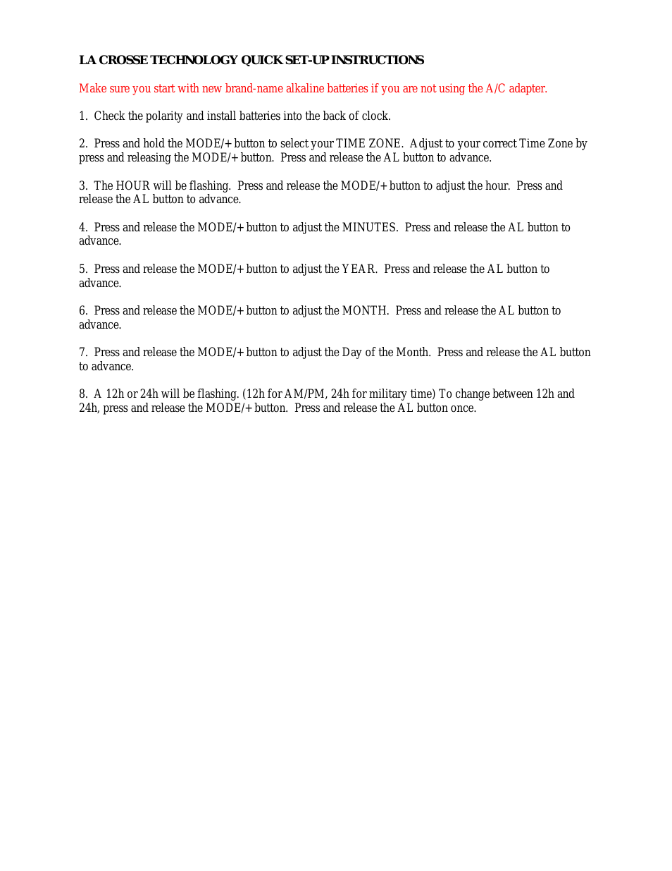
Table of contents
Document Outline
- Revision History
- Preface
- Table of Contents
- List of Figures
- List of Tables
- 1 Introduction
- Figure 1-1: PCI-9527 Product Image
- 1.1 Features
- 1.2 Applications
- 1.3 Specifications
- 1.3.1 Analog Input
- Table 1-1: Channel Characteristics
- Table 1-2: Crosstalk
- Table 1-3: Transfer Characteristics
- Table 1-4: Analog Input Channel Bandwidth
- Figure 1-2: Analog Input Channel Bandwidth, ±10 V Input Range
- Table 1-5: AC Coupling
- Figure 1-3: Magnitude Response of AC Couple of Input Channel
- Table 1-6: Integrated Electronic Piezoelectric (IEPE)
- 1.3.2 Analog Output
- 1.3.3 Triggers, Timebase
- 1.3.4 General Specifications
- 1.3.1 Analog Input
- 1.4 Software Support
- 2 Getting Started
- 3 Operation Theory
- 3.1 Functional Block Diagram
- 3.2 Analog Input Channel
- 3.3 Analog Output Channel
- 3.4 Trigger Source and Trigger Mode
- 3.5 ADC and DAC Timing Control
- 4 Calibration
- 5 Calibration
- Important Safety Instructions
Related manuals for Clock


New Manuals
- ZyXEL Communications ZyXEL G-162 Video Gaming Accessories User Manual
- ZyXEL Communications EW103U/A Video Gaming Accessories User Manual
- Western Telematic RSM-8 Video Gaming Accessories User Manual
- Western Telematic RSM-32DC Video Gaming Accessories User Manual
- Western Telematic RSM-32 Video Gaming Accessories User Manual
- Western Telematic RSM-16DC Video Gaming Accessories User Manual
- Western Telematic RSM-16 Video Gaming Accessories User Manual
- Viking Electronics FBI-1A Video Gaming Accessories User Manual
- Viking Electronics DVA-500A Video Gaming Accessories User Manual
- Viking Electronics DVA-3003 Video Gaming Accessories User Manual
- Viking Electronics DVA-2W Video Gaming Accessories User Manual
- Viking Electronics DVA- 1003B Video Gaming Accessories User Manual